“Observation of Polysilane by Near-field Scanning Optical Microscope for Ultraviolet Region”
Proc. ICL (Osaka, Aug.17 ,1999) (2000) 5–10.
M. Arai, S. Koshihara, M. Ueda, M. Yoshimoto, T. Saiki, S. Mononobe, M. Ohtsu, T. Miyazawa, and M. Kira
“Atomic-scale Control of Oxide Substrate Surface/Termination and Novel Heteroepitaxial Growth”
Mat. Res. Soc. Symp. Proc., Vol.587 (2000) O3.1.1 — 1.12.
M. Yoshimoto, K. Mizuno and T. Miyahara
“X-ray Photoelectron Spectroscopy Study of Hetero-interface Between Manganese Pnictclasse and Mn-Zn ferrite”
Jpn. J. Appl. Phys., Vol.39 (2000) 4486–4488.
T. Ikeda, H. Fujioka, K. Ono, M. Oshima, M. Yoshimoto and H. Koinuma
“Structural analysis of InxGa1-xN single quantum wells by coaxial-impact collision ion scattering spectroscopy”
Appl. Phys. Lett., Vol.77 (16) (2000) 2512–2514.
M. Sumiya, S. Nakamura, S.F. Chichibu, K. Mizuno, M. Furusawa, and M. Yoshimoto
“Effect of Al Pre-deposition Layer on the Epitaxial Growth of Silicon on Al2O3/Si(111) Substrates”
Thin Solid Films, Vol.369 (2000) 134–137.
M. Ishida, Y-C. Jung, H. Miura, Y. Koji, K. Sawada, M. Yoshimoto, K. Mizuno, T. Miyahara, and H. Maruta
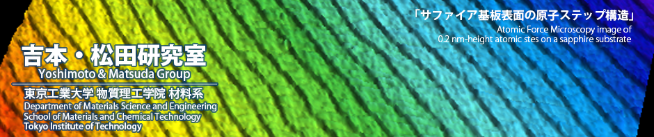
“Nanoscale Compsotion Analysis of Atomically Flat SrTiO3(001) by Friction Force Microscope”
J. Appl. Phys., Vol.88 (2000) 7099–7103.
K. Iwahori, S. Watanabe, M. Kawai, K. Mizuno, K. Sasaki, and M. Yoshimoto
“Homoepitaxial Growth Mechanism of ZnO(0001): Molecular Dynamics Simulations”
Phys. Rev. B, Vol.61 (23) (2000) 16187–16192.
M. Kubo, Y. Oumi, H. Takaba, A. Chatterjee, A. Miyamoto, M. Kawasaki, M. Yoshimoto, and H. Koinuma
“Amorphous silicon thin film transisters using MgO and Al2O3 gate dielectrics prepared by pulsed laser deposition”
Sci. and Tech. of Adv. Mater., Vol.1 (2000) 187–190.
N. Matsuki, M. Yoshimoto, J. Ohta, H. Fujioka, M. Ohshima and H. Koinuma
“Growth mode and surface morphology of GaN film deposited along the N-face polar direction on c-plane sapphire substrate”
J. Appl. Phys., Vol.88 (2000) 1158–1161.
M. Sumiya, K. Yoshimura, T. Ito, ,K. Ohtsuka, S. Fuke, K. Mizuno, M. Yoshimoto, H. Koinuma, A. Ohtomo and M. Kawasaki
“Influences of inert nitrogen molecu.les, nitrogen radical atoms and nitrogen molecular ions on growth process and crystal structure of GaN heteroepitaxial layers grown on Si(001) and Si(111) substrates by molecular beam epitaxy assisted by electron cyclotron resonance”
Proc. Int’l Workshop on Nitride Semicon. (IWN2000), IPAP Conf. Series 1 (2001) 351–354.
T. Yodo, H. Ando, H. Tsuchiya, D. Nosei, M. Shimeno, Y. harada, M. Furusawa and M. Yoshimoto
“Correlation between Optical Emission and Disordering of Indium in InxGa1-xN Single Quantum Wells Analyzed by Coaxial-impact Collision Ion Scattering Spectroscopy”
Proc. Int’l Workshop on Nitride Semicon. (IWN2000), IPAP Conf. Series 1 (2001) 575–578.
M. Sumiya, S.F. Chichibu, K. Mizuno, M. Furusawa, M. Yoshimoto and S. Nakamura
“Epitaxial growth of MnAs on single crystalline MnZn ferrite substrates”
J. Cryst. Growth, Vol.208 (2000) 395–400.
T. Ikeda, H. Fujioka, K. Ono, M. Oshima, M. Yoshimoto, H. Maruta, H. Koinuma, K. Inaba, and R. Matsuo